Research
 Nanoscale temperature mapping in operating microelectronic devices
Measuring temperature with very fine spatial resolution is extremely challenging. Contact thermometers must touch the sample, and thus tend to disturb its temperature. Non-contact pyrometers have their resolution limited by the wavelength of the thermal radiation that they detect. Here we describe a non-contact thermometry technique that has the best spatial resolution yet demonstrated (< 10 nm).
The technique, called plasmon energy expansion thermometry (PEET), works on the same principle as Fahrenheit's glass-bulb thermometer: materials expand or contract with temperature changes in a very predictable way. If you can measure a material's density with very high spatial resolution, you can measure temperature with high spatial resolution.
Implementing this reasoning, we capture temperature readings from fifty-thousand locations within a Joule-heated aluminum wire. PEET produces continuous maps, not scattered temperature readings from here and there. It returns temperatures in kelvin, not arbitrary units. Moreover, it does not require specialized, exotic, or custom hardware; the necessary equipment already exists in hundreds of laboratories worldwide.
We expect PEET to open lines of inquiry in the study of thermal transport that have long seemed intractable.

Nanofilament Formation and Regeneration During Cu/Al2O3 Resistive Memory Switching
The earliest computers were mechanical, with moving parts such as beads, gears and levers (e.g. the abacus, Babbage's analytical engine). With the development of the vacuum tube and the solid state transistor, computational machines became electronic. Surprisingly, technology is moving to complete the circle; next generation non-volatile memory is likely to involve atomic-scale mechanical switches that could do for ionics what the transistor did for electronics. These modern mechanical switches are known as ReRAM, or resistive random access memory.
This manuscript is the first report of time-resolved, nanometer-scale imaging of functioning ReRAM devices over numerous switching cycles. The nanopower devices imaged have no unrealistic interfaces or damage from sample preparation. They cycle many times instead of forming and then dying. The stages of the filaments development and disintegration are resolved into hundreds of time steps, not simply before and after. The filaments themselves are obvious in the data, and do not need to be pointed out with graphic indicators. Our real-time video data corroborate the standard model of filament formation, showing the filament growing backwards toward the active electrode.
Read the complete paper in Nano Letters.
Direct link to YouTube playlist: Nanofilament Formation and Regeneration During Cu/Al2O3 Resistive Memory Switching
Dark-field transmission electron microscopy and the Debye-Waller factor of graphene
Using first-principles quantum mechanics, we calculate the scattering of an electron beam from a one or several graphene sheets. The resulting simple analytic formulae agree well with dark-field images of few-layer graphene aquired in our transmission electron microscope.
We also calculate and measure the thermally-induced motion of the carbon atoms in a graphene sheet. This calculation shows that the oft-repeated statement "2D crystals are unstable" is completely false when applied to graphene. 2D crystals are thermally unstable only if they are larger than a certain size; for graphene this length scale is larger than the observable universe.
 In Situ Transmission Electron Microscopy of Lead Dendrites and Lead Ions in Aqueous Solution
Dendrite formation is a major problem for many battery chemistries, ranging from the one in your car (lead-acid) to the one in your smart phone (lithium-ion). The otherwise promising zinc-air battery chemistry is simultaneously inexpensive, high-capacity, and environmentally friendly, but it cannot be used in the most widespread energy distribution applications because dendrite formation prevents the construction of reliable rechargeable cells.
In our recent paper in ACS Nano we describe observing lead dendrite formation with a transmission electron microscope (TEM). This manuscript also presents the first electron-microscopy observations of solvated ions. The combination of TEM and fluid-filled environmental cells is thus capable of imaging both electrochemical products and reactants in real time, and should enable new insights into the critical problem of dendrite formation.
Read the complete article in ACS Nano.
Direct link to YouTube playlist: In Situ Transmission Electron Microscopy of Lead Dendrites and Lead Ions in Aqueous Solution
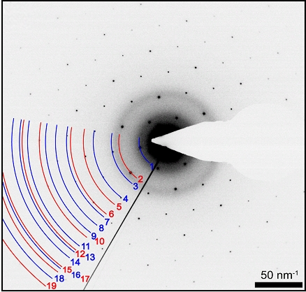
 Electron tomography at 2.4-ångström resolution
A series of 69 two-dimensional images of the nanoparticle was acquired using scanning transmission electron microscopy. In the course of this series the nanoparticle was tilted through a series of discrete angles, which provides the different perspectives necessary to perform the 3D reconstruction.
This technique is perhaps most famously implemented as a “CAT scan” for medical imaging with X-rays. We used a sophisticated algorithm called equally-sloped tomography (EST) for selecting the tilt angles, and invented a new method for aligning the projections using the “center of mass” of the images.
Read our letter published in Nature.
Read the UCLA press release | Read the California NanoSystems report | John Miao Group website
 Charged Nanoparticle Dynamics in Water Induced by Scanning Transmission Electron Microscopy
The properties of most functional biomolecules are determined by their charge interactions. With the development of environmental cells for use inside transmission electron microscopes (TEMs), high-resolution imaging of live biological specimens has recently become possible.
In this paper we demonstrate that, even at low intensities, the imaging electron beam can alter the charge state of particles under observation and thus dramatically influence the resulting dynamics. Charge effects induced by the electron beam in a TEM thus represent both a potential obstacle and a possible tool for studies of biological and other processes governed by the Coulomb interaction in water.
Read our published article in Langmuir.
Direct link to YouTube playlist: Charged Nanoparticle Dynamics in Water Induced by Scanning Transmission Electron Microscopy
 Single-color pyrometry of individual incandescent multiwalled carbon nanotubes
We image individual incandescent carbon nanotubes in an optical microscope and determine the absolute intensity of the light emitted at a 14 discrete wavelengths. Combining this data with measurements of the nanotube geometry acquired with a transmission electron microscope, we determine the temperature of the hottest portion of the nanotube using single-color pyrometry.
We also present an analytic solution to the non-linear one-dimensional heat equation that includes the temperature dependence of the thermal conductivity. We find that carbon nanotubes in vacuum fail due to sublimation around 2300 K. Furthermore, their thermal conductivity is still as large as 200 W/m K at this elevated temperature.
Read our published article in Physical Review B.
 Polarized light emission from individual incandescent carbon nanotubes
As nanotubes are quasi-one dimensional objects, it is natural to expect them to show polarization effects. Our manuscript presents polarization data on multiwalled carbon nanotubes with a level of detail that has not been seen previously. We use individual nanotubes as the filaments in tiny incandescent lamps, and image the light that they emit in both polarizations simultaneously.
Each nanotube has also been imaged in a transmission electron microscope, so its structure – namely length, diameter, core diameter, and number of walls – is well characterized at atomic length scales. We find that these devices consistently show a degree of polarization ~75%. This level of polarization is predicted by a classical model of the nanotube emissivity, where graphene’s optical conductance πα/Z0 is assigned to each nanotube wall.
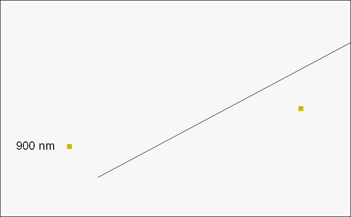 To the left the upper figure gives sequence of raw optical images showing how the light intensity in the two polarizations at a wavelength of 900 nm varies as the polarizing beam splitter is rotated through a full circle. When one spot is at maximum brightness and the other is at its minimum, one of the polarizer axes is aligned with the nanotube axis.
The lower figure shows a polar plot of one spot’s intensity: the radial coordinate represents light intensity, while the polar angle represents the corresponding polarizer orientation. The black line on this plot shows the direction of the nanotube axis as determined by the transmission electron microscope.
The excellent alignment between this axis and the emission pattern demonstrates that the polarized emission seen from the nanotube is determined by its orientation.
Read our published article in Physical Review B.
 Understanding the stability and dynamics of nanoscale bubbles
The Young-Laplace equation states that the pressure differential supported by a vapor-liquid interface scales like the surface tension divided by the interface’s radius of curvature. This well-established relation implies that the pressure inside a bubble increases towards infinity as the bubble radius decreases to zero. Such a seemingly unphysical result challenges us to better understand the stability and dynamics of nanoscale bubbles.
Previously very small bubbles have been studied with optical and atomic force microscopes, but neither of these techniques provides images of nanobubbles that are simultaneously high-resolution and unambiguous. Here we report the imaging of nanobubbles using scanning transmission electron micrcoscopy (STEM). We have constructed an electron-transparent, vacuum-tight cell that holds a few hundred nanometers of water sandwiched between two thin dielectric membranes.
By driving a current pulse through a platinum nanowire fabricated on one of the membranes we inject a small amount of heat into the water, forming a nanobubble that collapses when the power is removed. The images we capture with the electron microscope are among the best images of nanobubbles ever recorded.
Read our published article in APEX.
Direct link to YouTube playlist: Understanding the stability and dynamics of nanoscale bubbles
 Spin and the honeycomb lattice: lessons from graphene
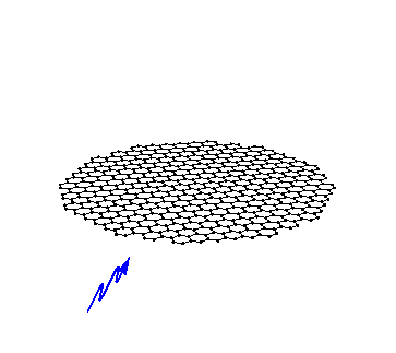
The standard cartoon of an electron shows a spinning sphere with positive or negative angular momentum, as illustrated in blue or gold to the left. However, such cartoons are fundamentally misleading: compelling experimental evidence indicates that electrons are ideal point particles, with no finite radius or internal structure that could possibly “spin.”
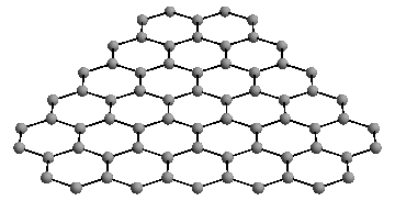
A quantum mechanical model of electron transport in graphene, a single layer of graphite (shown as a black honeycomb), presents a possible resolution to this puzzle. An electron in graphene hops from carbon atom to carbon atom as if moving on a chessboard with triangular tiles. At low energies the individual tiles are unresolved, but the electron acquires an “internal” spin quantum number which reflects whether it is on the blue or the gold tiles. Thus the electron’s spin could arise not from rotational motion of its substructure, but rather from the discrete, chessboard-like structure of space.
Read our published article in Physical Review Letters.
 Tree-level electron-photon interactions in graphene
Here we present the first fully quantum mechanical calculation of the interaction of light with graphene, a single layer of graphite. Our goal is to better understand how electron-hole recombination limits graphene transistor operation. This calculation reproduces beautiful results known previously; for instance, a suspended sheet of graphene absorbs (3.1415 a.k.a. Pi)* (the fine structure constant) = 2.3% of the light incident at right angles.
This remarkable result is seemingly independent of any graphene-specific properties, since Pi is a pure number and the fine structure constant depends only on fundamental constants describing the strength of the interaction between electrons and photons.) Our calculation also illuminates new features of the light-graphene interaction. It shows Ohm's law from an unusual vantage point: a graphene sheet, even one that is entirely defect-free and at zero temperature, can dissipate energy through the spontaneous emission of photons.
It also demonstrates that the angular dependence of polarized photon emission is influenced by the structure of graphene's honeycomb lattice. This connection between the graphene lattice and the photon polarization hints that the honeycomb structure is a source of angular momentum.
Read our published article in Physical Review B.
 Probing Planck’s Law with incandescent light emission from a single carbon nanotube
In this paper we report imaging the smallest incandescent lamp ever constructed. The filament, visible to the unaided eye when lit, appears as a tiny point of light since its length is comparable to the wavelength of the incandescent light it emits. Even our modern optical microscope barely resolves the filament’s non-zero length, since the light’s wavelength places a fundamental limit on the achievable optical resolution.
To “see” the filament, a single carbon nanotube, with atomic resolution we use an electron microscope (as opposed to a light microscope). In this way we can correlate the properties of the light emitted with the detailed molecular structure of the filament, which is only about 100 atoms wide. Our goal is to understand how Planck’s blackbody radiation law gets modified at small length scales. Planck’s law dates from 1900 and describes radiation from large, hot objects, such as a toaster, the Sun, or a light bulb.
Some such objects are of fundamental and current scientific interest; for instance, the thermal radiation left over from the Big Bang (called the cosmic microwave background) is described by Planck’s law. The carbon nanotube makes an ideal filament for this experiment, since it has both the requisite smallness, and the extraordinary temperature stability of carbon. In fact, Thomas Edison’s original light bulbs had carbon filaments.
Our light bulb is very similar, except that the filament is 100,000 times narrower and 10,000 times shorter, for a total volume only one one-hundred-trillionth of that of Edison’s version.
Read our published article in Physical Review Letters.
Press coverage: New Scientist | Slashdot | UCLA Newsroom | MetaEfficient | Physics World